

The clock is a bit of a Rubegoldberg machine but really it didn't have to be this way. All of the pain and annoyance of this particular project are entirely self inflicted, but once everything was debugged everything seemed to work as intended and nothing exploded of it's own accord. I helped it out with that a few times though.
That being said I've made a nixie clock. It powers the tubes from a spiral multiplier topology; if you're wondering what that is, see my last post cause I made it up and haven't seen it anywhere else. In this particular case it is a 4s3p multiplier array. This one in particular has 3 strands in parallel because it was easy to make a ring oscillator to drive them all out of phase, there is no other particular reason for it. Future designs could be done in a much more efficient compact fashion, that being said despite being an overly complex machine, it works. The FETs don't get hot at all, the caps are stressed a lot voltage wise but that was somewhat intentional and a bit of an experiment and you wouldn't notice if any of the supply was actually turned on and there's no noticeable noise, really nothing is being worked hard power wise.
The build up of the system went in a piece wise fashion. Multiplier was built up first, mainly because it was easy to free hand and capable of being treated as an independent lump with only a few connections.
 |
| First, assembly of the multiplier stack |
 |
| then the controllllls and inverter |
 |
| mooore soooooldering controls and inverter |
After making the multiplier came the PWM /controls set up. Since the system is open loop so there really aren't any controls to speak of. Controls would be logical for almost any other implementation, however the input to the multiplier system is a 15V regulated wall wart, and the multiplier itself is effectively a fancy step-up with constant load. So load variation and line variation are not issues. If people had the potential to plug in other regulators, or if the system were powered straight from the line regulation would be more of a concern. After finishing the inverter some basic testing was possible:
 |
| Single tube test of multiplier |
The multiplier is hiding in the far right f this picture, the inverter is front and center. Controls/ inverter are dead center. The Red wire is the HV into the tube. Output voltage from the supply can reach >200V with no load, but rides at 170V under load with all of the nixies. The voltage over the tube (that's on the multimeter) sits right at where the data sheets says it should site ~140V and in this test there was a resistor doing the current limiting for the tube. There are probably some resonant effects playing into the output voltage stability that I haven't characterized. The system output voltage is surprisingly invariant under different loads.
Feed back can always be added but, it wasn't needed and time, cost, effort...
 |
| It nibbles off the front end of the wave form and inverts it |
Six of these circuits were used, one for each pwm channel. They invert each wave and lop off the front of each pulse. Half of the delayed signals are inverted again. This makes it so there will be dead time between each pwming pair; and no shoot through between the hi and lo switches in each bridge.
 |
| Example of dead-time between falling and rising wave forms there is indeed something weird with the upperr wave form but I can't actually remember what is was anymore. |
 |
| Pretty Glowy Tubes |
The real regrets in this project (besides the assembly) comes with implementation of the digital controls for the clock. The power electronics were really the less obnoxious part, maybe that says something about my skill set, but at least I know why this part of the implementation was stupid and had an initial reason for the subsequent masochism. The digital controls comprises a clock chip, microcontroller, and load of stupid that fans out the microcontroller to all of the HV outputs. The clock chip is one of the cheapest through hole clock chips available the DS1307 by maxim. It's a pretty simple object and uses I2C to communicate with the microcontroller, this helps it keep actual accurate time with a crystal. One thing to note is that you can just buy a micro with a real time clock included, but this gave me an excuse to learn I2C. The microcontroller was an arduino, because as far as needing software or fancy programmers they represent an absolute minimum of effort and are acceptable for an application that doesn't have any respectable performance criteria.
`

For the fanout, eight digital outputs of the microcontroller are used to control all of the nixie tubes; effectively an 8 to 40 expansion as one switch is required to control each digit on each nixie tube. The size of the fanout was really somewhat annoying. The tubes have a comma digit to each side of the number that were left unused in this application. One thing to note is that technically access to all digits in each tube is not required; this was going to be a 24 hour clock making it so that only 3/10 available digits were used on the 10's hours digit...actually you could get away with 2/10 on the last digit if it was blanked instead of showing a '0' which would let you do everything with 32 outputs. But you could definitely do a 12 hour clock with 32 outputs. I'm getting away from crapping on the the current design which should have been implemented as a set of shift registers (or a single shift register). The fanout setup in the current system that was done for the following reasons:
A. to teach someone about human time vs. electrical time.
B. To have them consider the boundaries of what is required vs. what is optimal.
C. For some short amount of time it seemed like a fun idea.
A and B still seem like valid reasons. the fanout was set up as two channels of BCD, 4-digital pins of the micro went to each channel feeding one BCD which then fed 2 more BCDs from its 10 valid outputs. One set of three BCD for the minutes, another set for the hours.
This encoding and conversion was just annoying to deal with. There is one aspect missing here, because the first layer of the fanout can only select one output at a time, it can't produce all the combinations required on the output BCD's. To do this the following circuit was used:
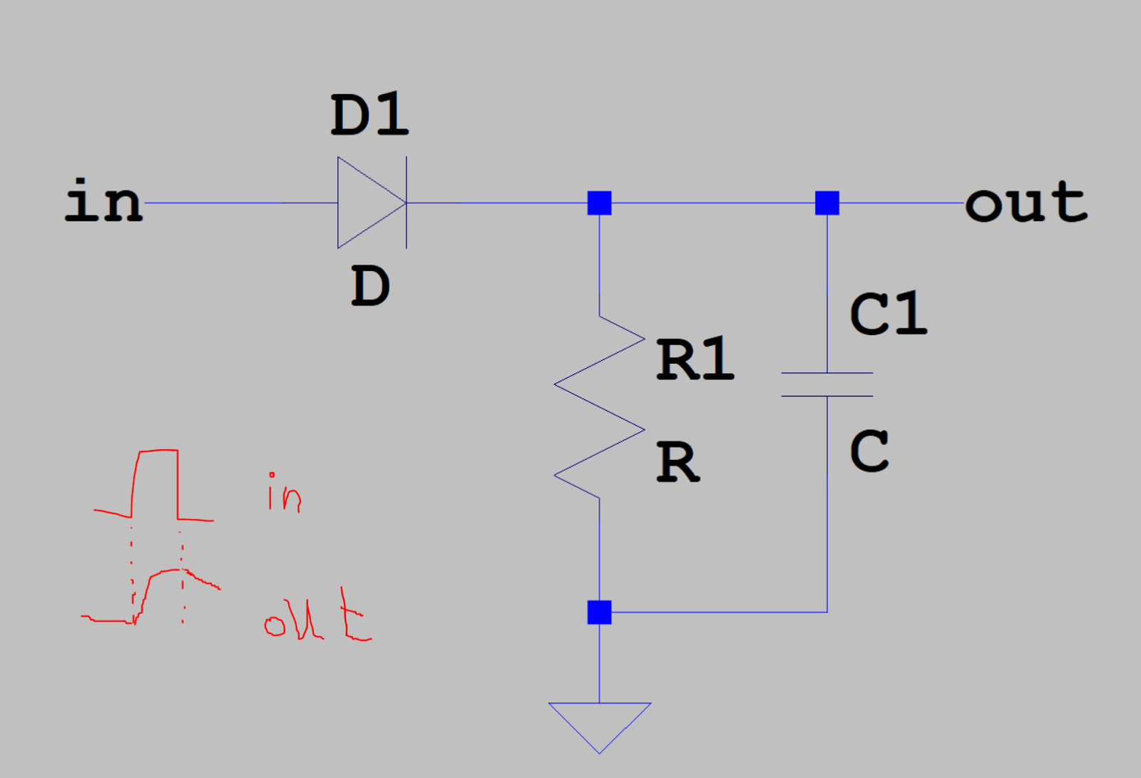
On the input of each second layer BCD the voltage is held by the RC. Then refreshed before the RC runs out. This allows the first layer BCD to turn on an arbitrary set of inputs to the second layer as long as its quick enough, which is pretty easy as long as the RC time constant is long enough. It's dumb but it seemed to work pretty well.
Finally after all these shenanigans the output of each second level BCD goes to a high voltage transistor for switching each digit on the tubes. This whole ordeal was far more trouble than it needed to be. But whatever, the clock clocks, and damn if those glowing tubes don't look pretty.
 |
| mmm glowy |
I bought a box to put the clock in as well, because not shocking people is important. That's less exciting, but I might make a post about it.
What's exciting though is I've already started on my next nixie venture and I'm most of the way done with it. It uses it's own silly topology and does not use any switching regulators to run off of the line, so you will be seeing a post about that.
No comments:
Post a Comment